- 您现在的位置:买卖IC网 > Sheet目录357 > SI8621ED-B-IS (Silicon Laboratories Inc)IC ISOLATOR 2CH 5KV 16-SOIC
Si8610/20/21/22
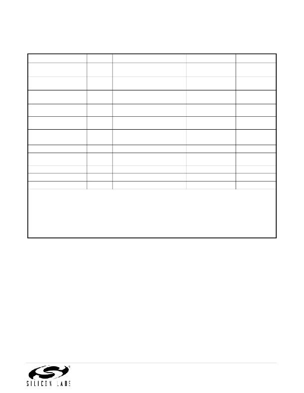
Table 3. Electrical Characteristics
(V DD1 = 3.3 V ±10%, V DD2 = 3.3 V ±10%, T A = –40 to 125 °C)
Parameter
VDD Undervoltage
Symbol
VDDUV+
Test Condition
V DD1 , V DD2 rising
Min
1.95
Typ
2.24
Max
2.375
Unit
V
Threshold
VDD Undervoltage
VDDUV–
V DD1 , V DD2 falling
1.88
2.16
2.325
V
Threshold
VDD Undervoltage
VDD HYS
50
70
95
mV
Hysteresis
Positive-Going Input
VT+
All inputs rising
1.4
1.67
1.9
V
Threshold
Negative-Going Input
VT–
All inputs falling
1.0
1.23
1.4
V
Threshold
Input Hysteresis
High Level Input Voltage
Low Level Input Voltage
V HYS
V IH
V IL
0.38
2.0
—
0.44
—
—
0.50
—
0.8
V
V
V
High Level Output Voltage
Low Level Output Voltage
Input Leakage Current
Output Impedance 1
V OH
V OL
I L
Z O
loh = –4 mA
lol = 4 mA
V DD1 ,V DD
2 – 0.4
—
—
—
3.1
0.2
—
50
—
0.4
±10
—
V
V
μA
?
Notes:
1. The nominal output impedance of an isolator driver channel is approximately 50 ? , ±40%, which is a
combination of the value of the on-chip series termination resistor and channel resistance of the output
driver FET. When driving loads where transmission line effects will be a factor, output pins should be
appropriately terminated with controlled impedance PCB traces.
2. t PSK(P-P) is the magnitude of the difference in propagation delay times measured between different units
operating at the same supply voltages, load, and ambient temperature.
3. Start-up time is the time period from the application of power to valid data at the output.
Rev. 1.4
9
发布紧急采购,3分钟左右您将得到回复。
相关PDF资料
SI8631EC-B-IS1
IC ISOLATOR 3CH 3.75KV 16-SOIC
SI8641ED-B-IS
IC ISOLATOR 4CH 5.0KV 16-SOIC
SI8652BD-B-IS
IC ISOLATOR 5CH 5.0KV 16-SOIC
SI8662EC-B-IS1
IC ISOLATOR 6CH 3.75KV 16-SOIC
SI9910DY-E3
IC MOSFET DVR ADAPTIVE PWR 8SOIC
SI9912DY-T1-E3
IC DRIVER GATE HALF BRIDGE 8SOIC
SI9976DY-E3
IC DRVR MOSF 1/2BRDG N-CH 14SOIC
SI9978DW-E3
IC FET DRIVER H-BRIDGE 1A 24SOIC
相关代理商/技术参数
SI8621ED-B-ISR
制造商:Silicon Laboratories Inc 功能描述:DUAL CH 5 KV ISOLATOR, 150M, 1/1, SOIC16, LEAD FREE (DEF OUT - Tape and Reel 制造商:Silicon Laboratories Inc 功能描述:IC ISOLATOR 2CH 5KV 16-SOIC 制造商:Silicon Laboratories Inc 功能描述:Dual Ch 5kV Isolator 150M
SI8621ET-IS
功能描述:General Purpose Digital Isolator 5000Vrms 2 Channel 150Mbps 60kV/μs CMTI 16-SOIC (0.295", 7.50mm Width) 制造商:silicon labs 系列:汽车级,AEC-Q100 包装:管件 零件状态:有效 技术:容性耦合 类型:通用 隔离式电源:无 通道数:2 输入 - 输入侧 1/输入侧 2:1/1 通道类型:单向 电压 - 隔离:5000Vrms 共模瞬态抗扰度(最小值):60kV/μs 数据速率:150Mbps 传播延迟 tpLH / tpHL(最大值):13ns,13ns 脉宽失真(最大):4.5ns 上升/下降时间(典型值):2.5ns,2.5ns 电压 - 电源:2.5 V ~ 5.5 V 工作温度:-40°C ~ 125°C 封装/外壳:16-SOIC(0.295",7.50mm 宽) 供应商器件封装:16-SOIC 标准包装:46
SI8622
制造商:SILABS 制造商全称:SILABS 功能描述:LOW-POWER SINGLE AND DUAL-CHANNEL DIGITAL ISOLATORS
Si8622BC-B-IS
功能描述:隔离器接口集成电路 2Ch 3.75 kV Isolator 150M 1/1 ADuM DO=LO
RoHS:否 制造商:Texas Instruments 通道数量:2 传播延迟时间: 电源电压-最大:5.5 V 电源电压-最小:3 V 电源电流:3.6 mA 功率耗散: 最大工作温度:+ 125 C 安装风格: 封装 / 箱体:SOIC-8 封装:Tube
SI8622BC-B-ISR
制造商:Silicon Laboratories Inc 功能描述:DUAL CH 3.75 KV ISOLATOR, 150M, 1/1, SOIC8, LEAD FREE, ADUM - Tape and Reel 制造商:Silicon Laboratories Inc 功能描述:IC ISOLATOR 2CH 3.75KV 8SOIC 制造商:Silicon Laboratories Inc 功能描述:Dual Ch 3.75 kV ISO 150M 1/1
Si8622BD-B-IS
功能描述:隔离器接口集成电路 Dual Ch 5kV Isolator 150M 1/1 ADuM, DO=LO
RoHS:否 制造商:Texas Instruments 通道数量:2 传播延迟时间: 电源电压-最大:5.5 V 电源电压-最小:3 V 电源电流:3.6 mA 功率耗散: 最大工作温度:+ 125 C 安装风格: 封装 / 箱体:SOIC-8 封装:Tube
SI8622BD-B-ISR
制造商:Silicon Laboratories Inc 功能描述:DUAL CH 5 KV ISOLATOR, 150M, 1/1, SOIC16, LEAD FREE, ADUM 12 - Tape and Reel 制造商:Silicon Laboratories Inc 功能描述:IC ISOLATOR 2CH 5KV 16-SOIC 制造商:Silicon Laboratories Inc 功能描述:Dual Ch 5kV ISO 150M
SI8622BT-IS
功能描述:General Purpose Digital Isolator 5000Vrms 2 Channel 150Mbps 60kV/μs CMTI 16-SOIC (0.295", 7.50mm Width) 制造商:silicon labs 系列:汽车级,AEC-Q100 包装:管件 零件状态:有效 技术:容性耦合 类型:通用 隔离式电源:无 通道数:2 输入 - 输入侧 1/输入侧 2:1/1 通道类型:单向 电压 - 隔离:5000Vrms 共模瞬态抗扰度(最小值):60kV/μs 数据速率:150Mbps 传播延迟 tpLH / tpHL(最大值):13ns,13ns 脉宽失真(最大):4.5ns 上升/下降时间(典型值):2.5ns,2.5ns 电压 - 电源:2.5 V ~ 5.5 V 工作温度:-40°C ~ 125°C 封装/外壳:16-SOIC(0.295",7.50mm 宽) 供应商器件封装:16-SOIC 标准包装:46
